
PIC32CM3204JH00032 Datasheet Core Specifications Overview: Master Key Parameters in 5 Minutes
In embedded system selection, the first page of the datasheet often determines whether engineers will proceed further. As a 32-bit MCU based on the Arm® Cortex®-M0+ core, the PIC32CM3204JH00032's core specifications directly impact the balance between low-power design and cost control. Based on the datasheet, this article distills six key parameter categories that must be understood within five minutes: core and frequency, memory capacity, power modes, peripheral interfaces, package size, and operating temperature range, helping you quickly assess during the evaluation phase whether the device meets your project requirements.
I. Product Positioning and Core Architecture of the PIC32CM3204JH00032
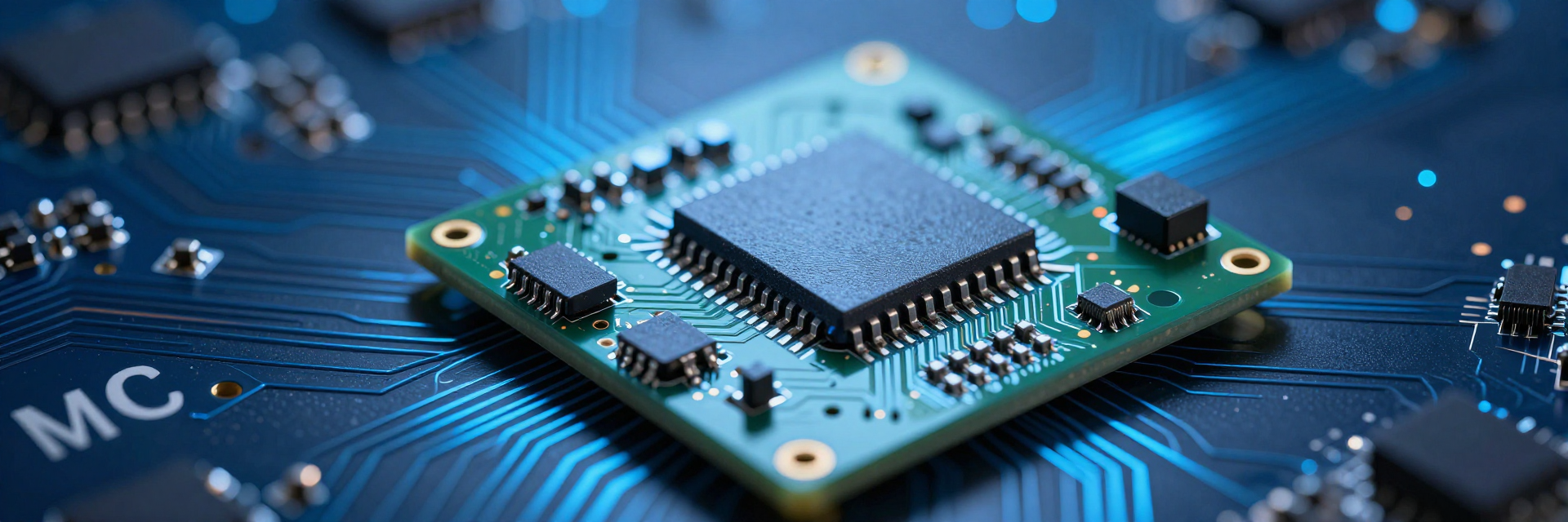
The PIC32CM3204JH00032 is positioned for general-purpose low-power embedded control applications. Its architectural design focuses on energy efficiency, making it suitable for high-volume applications that are sensitive to both cost and power consumption.
1.1 Core and Clock Frequency: Energy-Efficient Logic of Cortex®-M0+
This device uses the Arm Cortex-M0+ core with a maximum clock frequency of 48 MHz. The M0+ architecture achieves low power consumption per clock cycle through a two-stage pipeline and a reduced instruction set, delivering approximately 45 DMIPS of computing performance at 48 MHz, sufficient for tasks such as sensor aggregation, motor control, and communication protocol stacks.
1.2 Bus and Instruction Set: Single-Cycle I/O Access Mechanism
With single-cycle I/O port access and a microcontroller bus architecture, read/write latency to peripheral registers is significantly reduced, and interrupt response becomes more predictable. This mechanism is especially critical in applications requiring high-frequency GPIO toggling or rapid ADC triggering.
II. Quick Overview of Key Parameters in the Datasheet: Storage and Power Consumption
Storage and power consumption are the two pages with the highest information density in the datasheet, directly determining the upper limit of firmware size and battery life estimation.
2.1 Flash and SRAM Capacity Configuration
The PIC32CM3204JH00032 provides 64KB of Flash and 8KB of SRAM, supporting a storage architecture that allows simultaneous read and write operations, facilitating updates to parameter areas during runtime. For most bare-metal or lightweight RTOS applications, this capacity can accommodate protocol stacks and dual-backup configuration data.
2.2 Low-Power Mode Current Data Comparison
The typical current values listed in the datasheet are: approximately 2.5mA at 48MHz in run mode, about 1.2mA in idle mode, less than 5μA in standby mode, and less than 1μA in backup mode. When selecting components, calculate the average current weighted by your own wake-up duty cycle, rather than relying solely on the lowest value.
| Power Consumption Modes | Typical Current | Wake-Up Source |
|---|---|---|
| Run | 2.5mA | — |
| Idle | 1.2mA | Any interrupt |
| Standby | <5μA | External Interrupt/RTC |
| Backup | <1μA | RTC/Wake-up Pin |
III. Peripheral Interfaces and Pin Definitions Quick Reference
Peripheral resources determine system integration; reducing external components can compress the BOM and board area.
3.1 Communication Peripherals: SerCom and I²C/SPI/UART Allocation
The device integrates multiple SerCom modules, which can be flexibly configured as I²C, SPI, or UART. Combined with independent I²C and SPI interfaces, it meets bus requirements for coexisting sensors and wireless modules. When configuring, check the pin multiplexing table to avoid functional conflicts.
3.2 ADC Channels and Sampling Rate
The on-chip 12-bit ADC provides multi-channel inputs, and its sampling rate meets typical signal acquisition needs. The table in the datasheet showing the relationship between sampling time and source impedance is a core reference for precision design and should not be overlooked.
IV. Packaging and Operating Conditions: Hard Constraints During Selection
Package and electrical conditions are non-negotiable hard constraints that must be confirmed before the schematic stage.
4.1 Package Size and Pin Count
This model uses a 32-pin package, and the pin pitch and board footprint must align with the mechanical design. The pin count also limits the number of available GPIOs, so headroom should be reserved for debugging and expansion.
4.2 Temperature Grade and Supply Voltage Range
The operating temperature covers the industrial-grade range, and the supply voltage is 1.62V to 3.63V. The wide voltage range facilitates direct battery operation, but note the maximum clock frequency limitations at different voltages.
V. From Datasheet to Design Decisions: 3 Verification Steps
Translating datasheet data into design decisions requires a reusable verification process.
5.1 Parameter Verification Checklist
- Confirm that Flash/SRAM margin is no less than 30%
- Calculate average power consumption based on wake-up duty cycle
- Verify pin multiplexing and package board footprint
5.2 Common Misreadings and Pitfall-Avoidance Tips
Typical misreadings include treating standby current as average current, ignoring ADC source impedance requirements, and confusing the responsibility boundaries between the datasheet and the reference manual. It is recommended to define boundaries based on the datasheet and implementation details based on the reference manual.
The electrical tables in the datasheet are the starting point for design margin, not the endpoint of typical values.
Key Summary
- The PIC32CM3204JH00032 is based on the Cortex-M0+ core, with a 48MHz clock frequency that balances energy efficiency and computing power.
- 64KB Flash and 8KB SRAM meet the needs of lightweight protocol stacks and dual parameter backups.
- Standby current is below 5μA; average power consumption must be estimated using a weighted calculation based on wake-up duty cycle.
- SerCom offers flexible configuration for I²C/SPI/UART, and pin multiplexing should be verified in advance.
- A 32-pin package and a wide voltage range constitute strict selection constraints.
Frequently Asked Questions
What is the supply voltage range of the PIC32CM3204JH00032-I?
This device operates from 1.62V to 3.63V and supports direct battery operation. Note that the maximum clock frequency decreases as voltage drops; refer to the Electrical Characteristics table in the datasheet for specific conditions.
How can I estimate the average power consumption of the PIC32CM3204JH00032-I using the datasheet?
First determine the current in each mode and its duty cycle, then calculate a time-weighted sum. For example, if running at 10% and idle at 90%, the average current is approximately 0.1×2.5mA + 0.9×5μA, which is much lower than the active current.
Which parameters in the core specifications are most prone to misinterpretation?
Standby current is often mistaken for average current, and the relationship between ADC sampling time and source impedance is also easily overlooked. It is recommended to use the datasheet to define boundaries and consult the reference manual for detailed implementation.
What are the peripheral communication capabilities of the PIC32CM3204JH00032?
It integrates multiple SerCom modules that can be flexibly configured as I²C, SPI, or UART, and with independent interfaces, it meets the requirements of multi-sensor buses. When configuring, refer to the pin multiplexing table to avoid conflicts.