
In-Depth Analysis of the PIC32CM1216LE00032 Datasheet: Comprehensive Review of Specifications, Pinout, and Electrical Characteristics
When facing a datasheet that spans hundreds of pages, the most common dilemma faced by engineers is that critical specifications are scattered across different chapters, cross-referencing between pin definitions and multiplexed functions is complex, and test conditions within the electrical characteristics tables are easily overlooked. As a 32-bit MCU designed for low-power and security applications, the PIC32CM1216LE00032 datasheet conceals many design details that warrant in-depth interpretation.
This article adopts a data-driven approach to systematically break down the core specifications, pin architecture, and electrical characteristics of this chip, helping you establish a complete basis for component selection in the shortest possible time. Whether you are a hardware engineer or a firmware developer, mastering this three-tier screening logic will significantly enhance your component selection efficiency.
1. Chip Positioning and Overview of Core Specifications
1.1 Core Architecture and Memory Resource Configuration
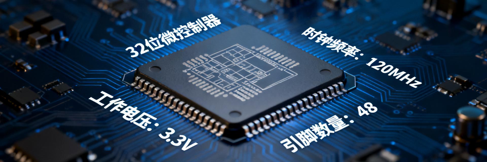
The PIC32CM1216LE00032 is based on the Arm Cortex-M0+ core with a maximum operating frequency of up to 48MHz, striking a balance between low power consumption and computational performance. It features 128KB of Flash memory, 16KB of SRAM, and is equipped with 2KB of data Flash for EEPROM emulation functionality.
It is worth noting that the cache and prefetch strategies of this chip directly affect actual execution efficiency. The wait-state table in the datasheet indicates that when the system clock exceeds 24MHz, 1 Flash wait state must be inserted, resulting in an approximate 5% performance penalty. It is recommended to enable the prefetch buffer during high-frequency operation to compensate for this.
1.2 Peripheral Integration and Functional Block Diagram Interpretation
This model integrates four 16-bit timers, three UARTs, two SPI and two I2C interfaces, as well as a 12-bit ADC (up to 12 channels). The functional block diagram shows that each peripheral communicates with the core via the APB bus, with the ADC and timers residing in different clock domains.
Compared to other models in the same family, the PIC32CM1216LE00032 falls into the mid-range configuration in terms of memory capacity, but features a lower pin count (32 pins), making it well-suited for space-constrained applications. The table below lists a comparison of key specifications:
| Parameter | PIC32CM1216LE00032 | High-End Model in Series |
|---|---|---|
| Flash | 128KB | 256KB |
| SRAM | 16KB | 32KB |
| Pin Count | 32 | 48 |
| ADC Channels | 12 | 16 |
2. Pin Definitions and Package Information Details
2.1 Pinout Diagram and Package Options
The PIC32CM1216LE00032 is available in QFN-32 (5x5mm) and LQFP-32 (7x7mm) packages. The pinout diagram is shown from a top-down view; note that pin 1 is located at the top-left corner of the package and arranged counter-clockwise.
Special attention should be paid to the layout logic of the power supply pins (VDD, VDDIO) and ground pins (VSS): an analog power supply (AVDD) and digital power supply (VDD) should be isolated via ferrite beads to avoid ADC sampling noise. The datasheet recommends placing a 100nF decoupling capacitor close to each power supply pin, paired with a 10μF bulk capacitor.
2.2 Pin Multiplexing Functions and Electrical Attributes
The GPIO multiplexing function table is the most frequently used section in the datasheet. Taking the PA0 pin as an example, its optional functions include: GPIO, UART0_TX, SPI0_MOSI, and ADC0. Quick localization method: first check the pinout diagram to confirm the physical pin number, then look up the corresponding peripheral column in the multiplexing function table.
The drive strength for each pin is divided into two levels: 4mA and 8mA, with the default reset state being high-impedance input. Special function pins such as the reset pin (RESET) require an external 10kΩ pull-up resistor, while clock input pins (XIN/XOUT) should be grounded or left unconnected when unused. Unused pins are recommended to be configured as low-level outputs or have internal pull-downs enabled to prevent leakage currents caused by floating states.
Section 3.2 of the datasheet clearly states: All unused pins should be configured by software as low-level outputs or externally connected via a 10kΩ pull-down resistor to ground, and must not be left directly floating.
Key Highlights
- The PIC32CM1216LE00032 adopts the Cortex-M0+ core, 48MHz frequency, 128KB Flash, and 16KB SRAM, making it suitable for low-power safety-critical applications.
- The pin multiplexing function table must be used in conjunction with the pinout diagram. Pins like PA0 feature multiple peripheral mappings, and drive strength and default states should be noted during configuration.
- In electrical characteristics, "typical values" are used for design calculations, while "maximum values" are used for limit verification; temperature derating has a significant impact on ADC accuracy.
- Unused pins must be handled properly; floating inputs can cause additional leakage currents, affecting overall power consumption performance.
- During component selection, key parameters strongly correlated with the application scenario should be locked in first, followed by verifying feasibility using the pin multiplexing and electrical characteristics tables.
Frequently Asked Questions
What factors affect the ADC accuracy of the PIC32CM1216LE00032?
ADC accuracy is primarily influenced by reference voltage stability, sampling time, and temperature. The datasheet shows that over the -40°C to 85°C range, the typical integral nonlinearity (INL) error of the 12-bit ADC is ±2 LSB, with a maximum of ±4 LSB. It is recommended to use an external voltage reference source and ensure the sampling time is greater than 1μs.
How to quickly find all multiplexed functions of a specific pin on the PIC32CM1216LE00032?
First, consult the pinout diagram to confirm the physical pin number, then locate the corresponding row in the multiplexing function table and read across the peripheral columns. Note that a "-" in the table indicates that the pin does not support that function. It is recommended to organize commonly used pin functions into a table for quick reference during design.
What is the power consumption performance of the PIC32CM1216LE00032 in low-power modes?
The datasheet specifies a typical current of 1.2mA in Sleep mode, which can drop down to 15μA in Deep Sleep mode (with RAM and RTC retained). Regarding wake-up time, waking up from Deep Sleep takes approximately 20μs. Actual power consumption is affected by peripheral configuration and pin states, and clocks for unused peripherals should be disabled.
How should typical and maximum values in the electrical characteristics table of the datasheet be used?
Typical values are used for design calculations and power consumption estimations under typical operating conditions, while maximum values are used to ensure the system operates correctly under worst-case conditions. At least a 20% design margin should be reserved during component selection, taking temperature derating into account. Exceeding recommended operating conditions may lead to parameter drift or device damage.