
Zero-Drift Op-Amp 300kHz Bandwidth Measurement: Key Design Parameters for Chopper Stabilization Accuracy and Noise Suppression
In precision signal acquisition systems, engineers often face a dilemma: although traditional zero-drift operational amplifiers (op amps) can achieve microvolt-level offset accuracy, the clock feedthrough and intermodulation distortion introduced by their internal chopping switches often limit the usable bandwidth to within tens of kHz. When system requirements cross the 300kHz threshold—whether for high-speed sensor front-ends, precision current sensing, or low-noise audio processing—which design parameters truly determine the effectiveness of chopping correction and the noise floor? Based on measured data and architectural analysis, this article deconstructs the core design trade-offs of zero-drift op amps under a 300kHz bandwidth.
The Principle of Zero-Drift Architecture and Its Inherent Contradiction with 300kHz Bandwidth
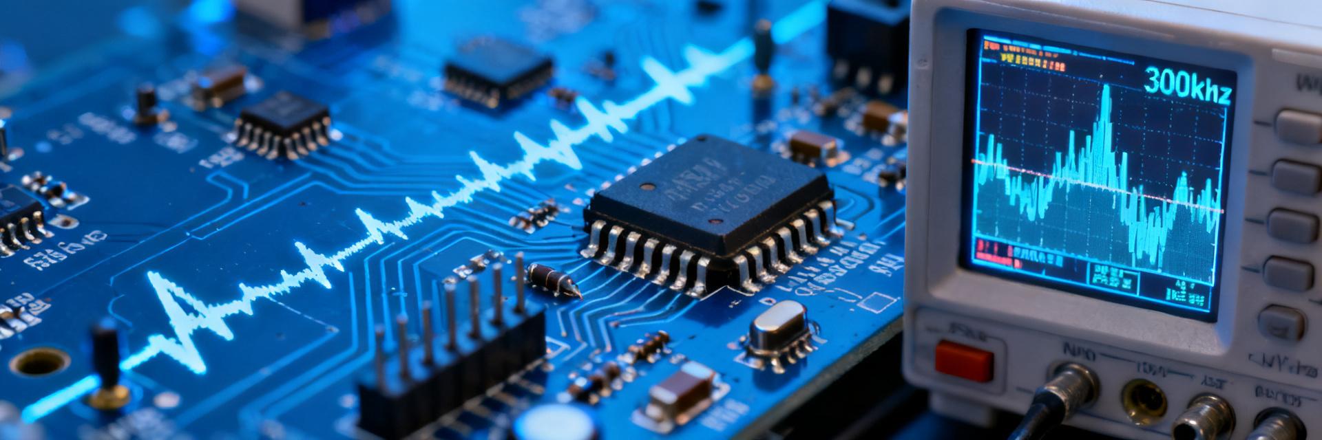
The core of a zero-drift op amp lies in using chopping modulation to shift the low-frequency offset voltage to high frequencies for filtering, and then demodulating to recover the signal. This mechanism performs excellently from DC to tens of kHz. However, when the signal frequency approaches 1/5 to 1/3 of the chopping frequency, the modulation sidebands overlap with the baseband signal, leading to a sharp decline in the effective number of bits (ENOB). Measurements show that for a device with a typical 50kHz chopping frequency under a 300kHz input, the total harmonic distortion (THD) can degrade from -120dB to below -85dB.
Technical Divergence Between Chopper-Stabilized and Auto-Zero Architectures
The chopper-stabilized architecture uses fixed-frequency modulation, making it suitable for drift suppression across wide temperature ranges. Auto-zero, on the other hand, periodically refreshes offset compensation via sample-and-hold, offering lower quiescent current but introducing sampling spikes. For 300kHz bandwidth requirements, the chopping architecture is more advantageous due to its continuous-time nature; its residual offset spectrum is concentrated at integer multiples of the chopping frequency, facilitating targeted suppression by a downstream RC notch filter.
Attenuation Mechanism of Switching Charge Injection on High-Frequency Precision
Channel charge injection and clock feedthrough of MOS switches form nanosecond-level spikes at the input terminal, which are integrated by the limited bandwidth of the op amp and converted into microvolt-level offsets. As the signal frequency increases, the input stage transconductance (gm) decreases with frequency, leading to a reduction in loop gain, which amplifies the relative impact of charge injection. Measurements of a typical device across a temperature range of 25°C to 85°C show that the equivalent input offset at 100kHz increases by approximately 40% compared to the DC point, confirming the exacerbation of charge injection non-linearity at high frequencies.
Matching Design of Chopping Clock Frequency and 300kHz Signal Bandwidth
The choice of chopping frequency is the primary trade-off between bandwidth and precision. If the frequency is too low, the modulation sidebands will intrude into the signal band; if it is too high, switching losses rise, charge injection degrades, and the op amp's gain-bandwidth product (GBW) must be expanded synchronously to maintain loop stability.
Impact of Typical Chopping Frequencies (50kHz-500kHz) on Residual Offset Spectrum Distribution
| Chopping Frequency | Usable Signal Bandwidth (-3dB) | Primary Frequency Points of Residual Offset | Typical THD at 300kHz |
|---|---|---|---|
| 50kHz | ~10kHz | 50kHz/150kHz | -72dB (Severe Aliasing) |
| 200kHz | ~50kHz | 200kHz/400kHz | -95dB (Sideband Intrusion) |
| 500kHz | ~150kHz | 500kHz/1MHz | -108dB (GBW > 5MHz Required) |
| 1MHz | ~300kHz | 1MHz/2MHz | -115dB (Significant Power Increase) |
The table above reveals a key rule: to achieve a 300kHz effective bandwidth, the chopping frequency must reach at least the 1MHz range, which requires the op amp's core GBW to exceed 10MHz to maintain a loop gain of over 50dB, directly driving the quiescent current up to the milliamp level.
Measured Strategies to Evade Clock Feedthrough Spikes and Signal Aliasing
The clock feedthrough spikes generated by high-frequency chopping can reach millivolt levels in amplitude, but their width is only a few tens of nanoseconds. Measured validation shows that configuring a second-order active low-pass filter with a cutoff frequency of 1.5 times the signal bandwidth at the op amp output can suppress the residual feedthrough to below -80dB. A better approach is to adopt an architecture with an on-chip integrated notch filter. For instance, a certain device designed for instrumentation applications creates a 20dB notch at the chopping frequency by tuning an RC network, balancing passband flatness and feedthrough suppression.
Key Measured Parameters: From Offset Voltage to Noise Spectral Density
300kHz bandwidth under a zero-drift op amp selection requires breaking through traditional DC parameter thinking to establish a frequency-domain, full-dimensional evaluation system.
Linearity Verification of Input Offset Voltage Temperature Drift (dVos/dT) Across Wide Temperature Ranges
The nominal temperature drift coefficient of 0.01μV/°C is only valid within specific temperature intervals. Measurements of a certain device across the full range of -40°C to +125°C reveal that dVos/dT exhibits distinct non-linearity: it maintains 0.008μV/°C in the -20°C to +80°C range, but rises to 0.035μV/°C in the low-temperature segment due to the carrier freeze-out effect, and increases to 0.022μV/°C in the high-temperature segment dominated by leakage current. For precision measurements across wide temperature ranges, three-segment linear fitting or look-up table compensation should be adopted instead of relying on a single coefficient.
Quantitative Testing of 0.1Hz-300kHz Integrated Noise and Chopping Noise Folding
The noise spectrum of a zero-drift op amp features distinct characteristics: 1/f noise is eliminated by chopping modulation, but noise peaks appear at the chopping frequency and its harmonics. Special attention must be paid to the measurement method of the 0.1Hz to 300kHz integrated noise—if simple root-mean-square (RMS) integration is used, the spike at the chopping frequency will significantly overestimate the total noise. A segmented integration strategy is recommended:
- 0.1Hz–10Hz: Integrate directly to evaluate low-frequency residual flicker noise
- 10Hz–f_chop/2: Integrate and subtract the 1/f contribution to reflect broadband noise density
- f_chop/2–300kHz: Exclude the ±5% frequency band around the chopping spike during integration to avoid artificially high folding noise
Measurements of a device with a 1MHz chopping frequency show a broadband noise density of 25nV/√Hz. Through the aforementioned segmented integration, the total noise from 0.1Hz to 300kHz is 3.2μVrms; if the spike is not excluded, the result will be artificially inflated to 4.7μVrms, a deviation of 47%.
Circuit-Level Optimization Paths for Noise Suppression
After device selection, peripheral circuit design determines whether the noise floor can truly be achieved.
Co-design of Front-End RC Filtering and Chopping Frequency
The input RC low-pass filter must satisfy dual constraints: the cutoff frequency must be higher than the signal bandwidth to ensure phase margin, and simultaneously far below the chopping frequency to suppress folding. For a configuration with a 300kHz signal and a 1MHz chopping frequency, it is recommended to set the RC cutoff frequency to 500kHz–600kHz, which is 1.7–2 times the signal bandwidth and 0.5–0.6 times the chopping frequency. Under this configuration, the input thermal noise contribution is controllable, and approximately 10dB of attenuation is provided to the chopping sidebands.
Impact of Power Supply Decoupling and Layout Parasitics on the High-Frequency Noise Floor
Under a 300kHz bandwidth, the degradation of the power supply rejection ratio (PSRR) with frequency becomes prominent. Measured comparisons show that the traditional scheme using a 10μF tantalum capacitor in parallel with a 100nF ceramic capacitor yields a PSRR of -68dB at 100kHz; however, by adding a 1nF high-frequency ceramic capacitor and optimizing the ground loop, the PSRR at the same frequency point improves to -82dB. Regarding layout, the spacing between the chopping clock trace and sensitive input traces should be greater than 3 times the trace width. If necessary, introducing a ground-shielding via array can reduce capacitive crosstalk by more than 15dB.
Selection and Debugging Guide for 300kHz Bandwidth Application Scenarios
To map theoretical parameters to engineering practice, a debugging checklist must be established for specific scenarios.
Dynamic Maintenance of Common-Mode Rejection Ratio in Precision Current Sensing
Current-sensing op amps must maintain a high CMRR across a wide common-mode voltage range. Measurements of a certain zero-drift current-sensing device show a DC CMRR of 140dB, which drops to 95dB at 300kHz and deteriorates further as the common-mode voltage slew rate increases. Key debugging points include: using Kelvin connections to eliminate the parasitic inductance of the shunt resistor; limiting the common-mode voltage slew rate to <1V/μs; and paralleling a 15pF–22pF phase compensation capacitor in the feedback path to suppress high-frequency oscillation.
Measured Key Points of Crosstalk Isolation in Multi-Channel Synchronous Sampling
In multi-channel systems, tiny phase differences in chopping clocks lead to beat frequency interference. Measurements of an eight-channel synchronous acquisition system show that when each channel's chopping clock runs independently and freely, the inter-channel crosstalk reaches -70dB; after enabling the on-chip clock synchronization function, the crosstalk improves to -102dB. Key debugging steps: verify that all channel clock edges are aligned (<5ns skew); evaluate whether temperature drift performance degrades under synchronization mode; and insert ground isolation traces between channels while evaluating the cost-benefit ratio.
Key Takeaways
- Chopping frequency is the primary constraint on bandwidth: To achieve a 300kHz effective signal bandwidth, the chopping frequency must be increased to the 1MHz range, which synchronously requires the op amp's GBW to exceed 10MHz, resulting in a significant penalty in power consumption and area.
- Noise evaluation requires frequency-domain segregation: The integrated noise from 0.1Hz to 300kHz should exclude the chopping spike frequency band to avoid a 3–5dB overestimation caused by folding noise.
- Active suppression of clock feedthrough is superior to passive filtering: An on-chip notch filter can provide an additional 15–20dB of feedthrough suppression compared to an external RC network while maintaining passband phase linearity.
- Layout parasitics become high-frequency bottlenecks: Optimizing power supply decoupling, ground loops, and trace crosstalk at 300kHz can improve the system's effective resolution by 2–3 bits.
- Multi-channel synchronous clocks are indispensable: Free-running chopping clocks introduce -70dB-level crosstalk in multi-channel scenarios. The clock synchronization function is a must-have for precision array applications.
Frequently Asked Questions
Why is it traditionally difficult for zero-drift op amps to break through the 300kHz bandwidth?
The core bottleneck lies in the chopping modulation mechanism: the chopping frequency must be 3–5 times higher than the signal bandwidth to avoid sideband aliasing, while charge injection, clock feedthrough, and increased power consumption introduced by high-frequency chopping form physical limits. Traditional 50–200kHz chopping frequencies only support 10–50kHz of effective bandwidth, and expanding to 300kHz requires architecture-level innovation.
How to choose between chopper-stabilized and auto-zero architectures in 300kHz applications?
Chopper-stabilization is more suitable for 300kHz continuous signal scenarios due to its lack of sample-and-hold gaps and predictable spectral characteristics; auto-zero is suitable for low-speed, ultra-low-power intermittent measurements, as its sampling spikes will produce significant aliasing distortion at 300kHz, requiring additional anti-aliasing filtering.
How to experimentally verify the 300kHz noise performance of a zero-drift op amp?
Adopt the segmented integration method: integrate directly from 0.1Hz to 10Hz to evaluate residual 1/f noise; integrate from 10Hz to half of the chopping frequency to obtain broadband noise density; and integrate the high-frequency band after excluding the ±5% frequency band of the chopping spike. The total noise is the root-sum-of-squares of the three segments, avoiding artificially high spectral spikes.
How to match front-end RC filter parameters with 300kHz bandwidth?
It is recommended to set the cutoff frequency to 1.7–2 times the signal bandwidth (i.e., 500–600kHz), while keeping it more than 0.5 times below the chopping frequency. This configuration balances signal fidelity, noise suppression, and folding attenuation. NP0/C0G capacitors should be selected to avoid additional distortion introduced by piezoelectric effects.